Editor’s note: This post is by P99 CONF 24 speaker Jason Rahman (Principal Software Engineer at Microsoft). Jason will be talking about “Scheduler Tracing With ftrace + eBPF.” Understand app latency by exploring the Linux scheduler with ftrace, eBPF, and Perfetto for visualization. Jason will share quirks in the CFS scheduler and provide a glimpse of the new EEVDF scheduler in recent kernels.
To read more from Jason, follow his Substack newsletter, Delayed Branch: Adventures In Low Level Programming And Software Development.
***
Over the past 10-15 years, per-core throughput increases have slowed, and in response CPU designers have scaled up core counts and socket counts to continue increasing performance across generations of new CPU models. This scaling however is not free. When scaling a system to multiple sockets using NUMA (Non-Uniform Memory Access), software must generally take the NUMA topology and locality into account.
However, there is a second level of locality present in more recent, high core count systems which many overlook. To scale to higher core counts, these high core count CPUs implement a Network-On-Chip (NOC) interconnect within each physical CPU die and package, typically some sort of mesh or ring bus, to communicate between CPU cores (or more precisely, between L3 cache slices and L2 + L1 caches associated with each core) on the same physical CPU die. Depending on the particular topology used for the network, the interconnect will have varying performance characteristics.
For most applications and CPUs, these performance differences will be negligible in practice for all but the most demanding workloads. However, they are detectable with microbenchmarks. And moreover, certain CPU models do have noticeable performance impacts at the application level if the non-uniformity in communication costs between cores on a physical CPU package is neglected.
To begin, we’ll look at a pair of Intel CPUs, and observe a few key details on their on-die interconnect topology and impact on cross-core communication patterns. In a subsequent post we’ll take a look at AMD Rome and AMD Milan CPUs, and their much more nuanced hierarchy.
Measurement Methodology
All measurements are performed on bare metal EC2 instances running in AWS. Bare metal whole host instances were used to avoid interference from co-located workloads on the same host given the sensitive nature of these measurements. You can find the tool used to perform these measurements on Github here: https://github.com/jrahman/cpu_core_rtt.
Intel Monolithic Topology
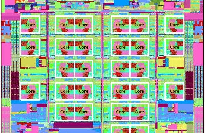
The Intel CPUs we’ll take a look at today are both monolithic dies with 24 to 32 cores per CPU socket. The diagram below shows the general layout for these dies:
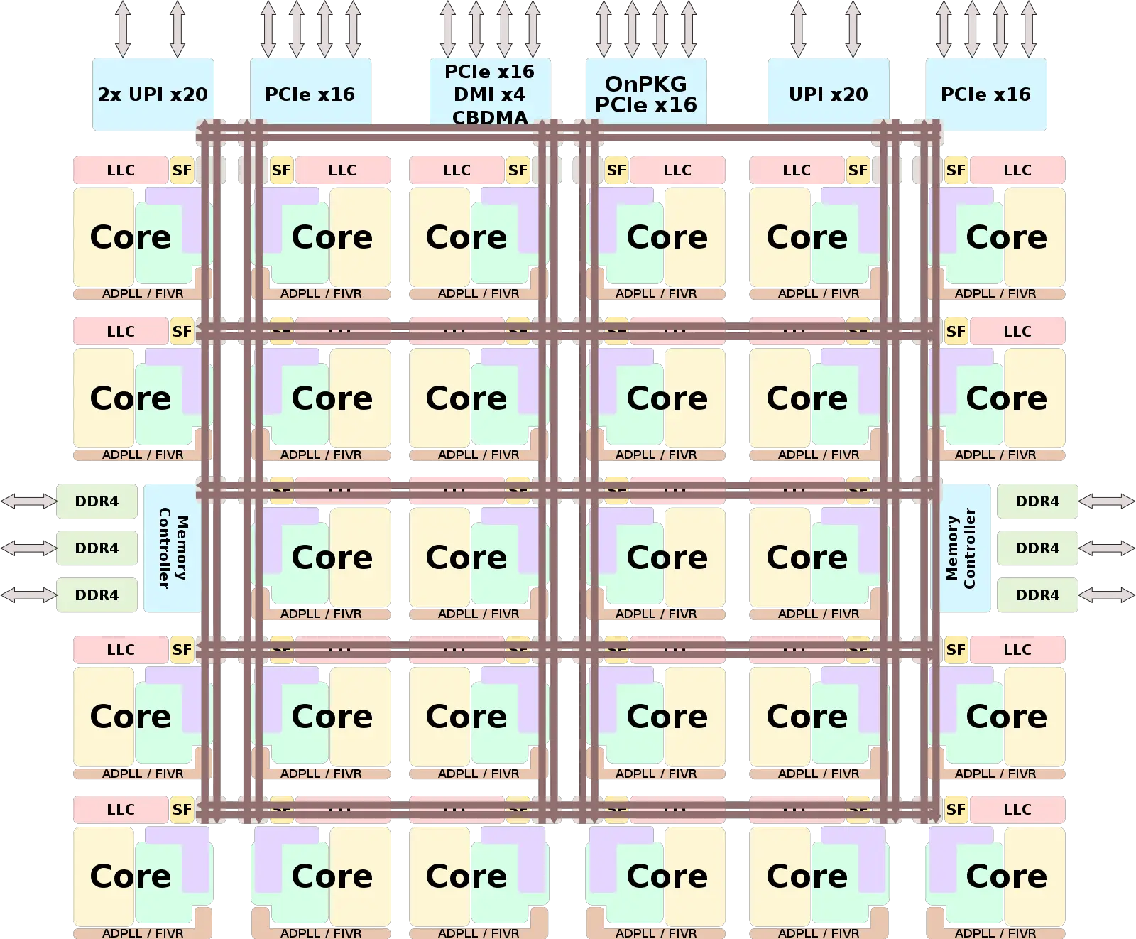
A few points to note. The mesh interconnect is clearly shown in the diagram. Each CPU core (including both Hyperthreads) has a Caching and Home Agent (CHA in Intel documentation). The L3 cache for the die is divided into multiple “slices”, with one slice attached to each CPU core. The L3 cache slice attached to a core is not exclusive to that particular CPU core. Rather, any CPU core on the same physical die has equal access to any L3 cache slice elsewhere on the die by sending messages over the mesh interconnect. The CHA is connected to the mesh interconnect as a network stop. Accesses to the L3 slice are from other CPU cores mediated through the Caching/Home Agent, as are outbound messages from the attached CPU cores.
With that conceptual background out of the way, let’s look at a couple examples of the mesh interconnect’s performance.
Cascade Lake
First up, our dual socket Cascade Lake system. This particular system is a c5.metal AWS instance with two 24 core (48 thread) Xeon Platinum 8275CL CPUs. The 24 core Cascade Lake SKUs running in AWS are based on the XCC die, nominally with 28 cores, but running with 4 of those cores fused off (likely for yield and TDP reasons).
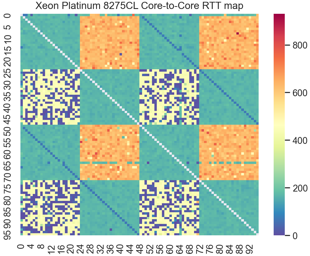
The diagram above shows the mesh topology used in the Cascade Lake XCC die. The worse case for core-to-core communication would be a 18 hop round trip between CPU cores on opposite corners of the silicon die.
The heatmap clearly shows a some key details. First, the NUMA cost is clearly apparent. The orange/red/yellow squares represent pairs of cores on different NUMA nodes. There is at least a 5-10x penalty when communicating with a CPU core on a different NUMA node. And this is one a dual socket system with only a single NUMA hop. Higher NUMA factor systems can incur multiple node hops.
We also see the Hyperthreads show up as the blue diagonals. Those CPU cores communicate through a shared L1 cache, instead of communicating across the mesh interconnect within the CPU die, or across the UPI interconnect between CPU sockets.
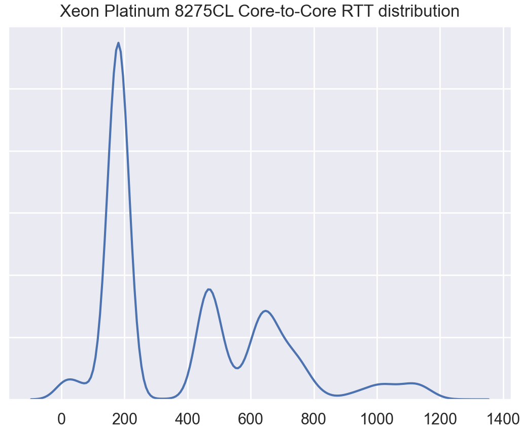
The histogram show a few different modes, a small peak at the far left edge is from the low latency RTT between Hyperthreads on the same physical CPU core, while the primary peak around 200 ticks represent on-die communication through the ring interconnect. The rest of the peaks reflect cross NUMA node over the UPI cross-socket interconnect.
Ice Lake
Next up, we have a dual socket Ice Lake system. This is a AWS c6i.metal host running dual Xeon Platinum 8375C CPUs, each with 32 physical CPU cores and 64 hyperthreads for a total of 64 cores + 128 threads.
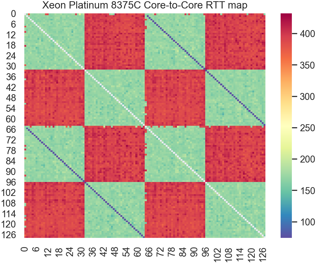
The latency heatmap already shows a very flat and consistency latency profile. Just like the Cascade Lake data, we observe the Hyperthread pairs show up as partial diagonals. While the separate NUMA nodes show up clearly. Green squares reflect RTT time between cores on the same NUMA node, while longer RTTs between CPU cores running on different NUMA nodes show up as higher RTT red squares.
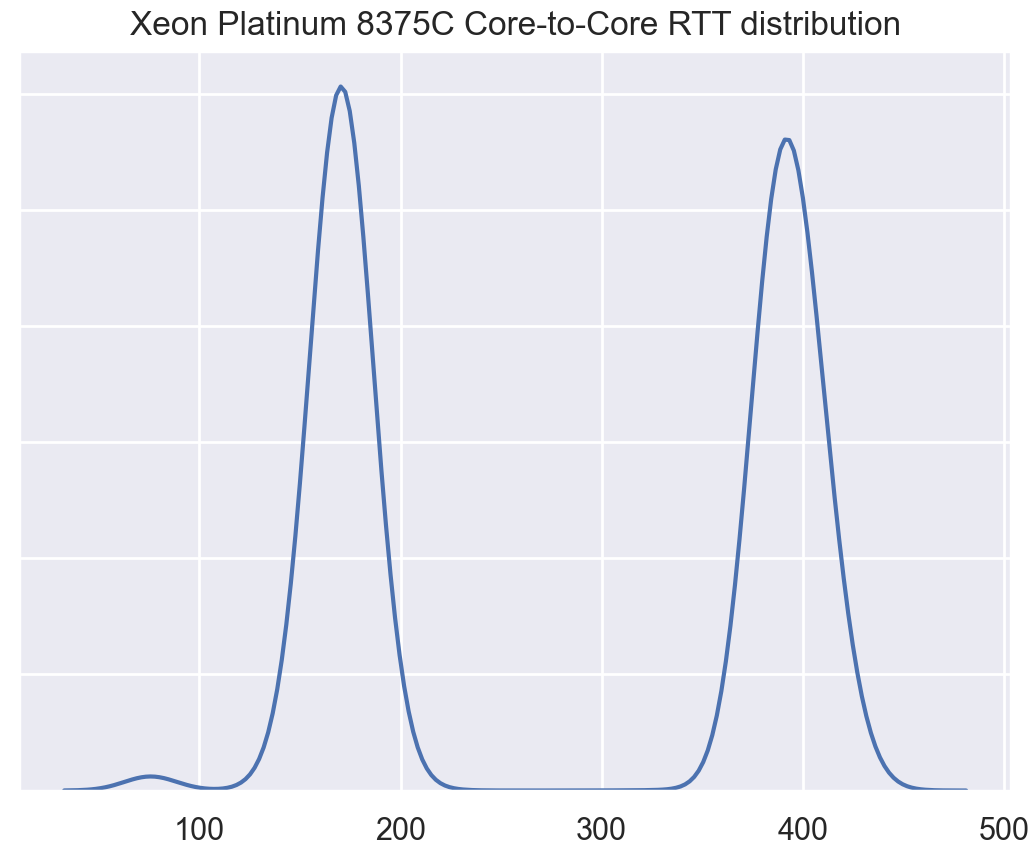
The above histogram also shows the clear triple peak, revealing, from left to right:
- Low hyperthread to hyperthread RTT around ~50 ticks
- Within die mesh interconnect RTT around 175 ticks
- Cross NUMA node UPI interconnect RTT around 400 ticks
Compared to Cascade Lake, we see from both the histogram and the latency heatmap, that Ice Lake has tightened up the latencies between cores within the same die. While some of the differences here may be measurement noise, it appears that after a few generations using a mesh interconnect (starting with Skylake) Intel has clearly been making solid generation over generation improvements.
Conclusions + Next Round
We’ve seen the fairly flat latency profile which Intel’s on-die mesh interconnect yields. While the histograms do reveal some amount of variance in communication cost, that variance is quite low, and newer generations have fairly predictable and flat latency profiles across the CPU die. For practical purposes, on Intel CPUs, nearly all software can treat the communication cost across cores as both uniform, and low enough to generally not show up as a performance issue.
Next up we cover AMD CPUs, both Rome (Zen 2) and Milan (Zen 3), which (spoiler) do have noticeable variation in communication costs within a CPU package.

